|
|
||||
|
Iwai Laboratory
Frontier Research Center, Tokyo Institute of Technology TEL:+81-45-924-5471 FAX:+81-45-924-5584  Last Update:28th September, 2009 |
(the Most Advanced CMOS)
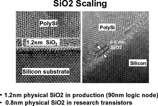
 gate length: 30nm gate insulation film: 0.8nm diffusion layer: 20nm [High-k materials] ZrO2, HfO2, La2O3, CeO2 Na2O3, Sm2O3, Eu2O3,Gd2O3 Tb2O3, Dy2O3, Ho2O3, Er2O3 Tm2O3, Yb2O3, Lu2O3 > Research plan Close cooperation with the industrial world > Domestic technical tie-up STARC, Toshiba, Nichiden, Hitachi, Sanyo, Matsushita, Denso > International joint research LEIT and LPCS in Flance, and NCSU in U.S.A. > Experiment equipment [ISE&SILVACO] This is the workstation equipping TCAD6.1 of ISE, the comprehensive device simulator which is available of process simulation to device simulation.Also, the workstation equips SmartSpice and Utmost3 of SILVACO. It can analize circuits and extract the parameter of a simulation model. [MBE]   MRE is possible to deposit pure thin films among a super-high vaccum(-10-10Torr).The device equips four E-guns, and can deposit two kinds of thin films simultaneously. Now, it is used in order to deposit an oxide. [Measurement equipment]  It is the measurement system which measure almost all electrical properties:the main equipments are PUROBA, 4156A, 4284A, etc). The nickname is "doghouse". |
|||
